|
TASK – FULL ADDER TASK DESCRIPTION We have seen a half adder circuit which adds two bits together. However, to add multi-bit numbers together,
the half adder is not quite enough. In this circuit, we will look at how to create a full adder. Using n full adders together, we can add up
two n bit numbers. THEORY PART 1 – WHY DOESN’T A HALF ADDER
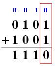
WORK? Consider the addition of
two multi-bit binary numbers.
Essentially, we are
adding each column up individually taking into consideration the carry over
from the previous addition. So each column addition
actually needs three inputs: the carry in from the previous column, and the
two bits. The half adder on its
own cannot handle the carry in bit so we need to create another circuit. PART 2 – THE FULL ADDER’S TRUTH TABLE It has three inputs -
the two numbers in question and the carry over from the previous
addition. It has two outputs – the
sum that appears at the bottom of the addition and the carry out that will be
added in the next column’s addition. For the full adder, the
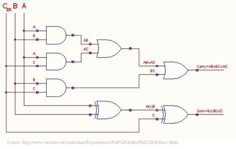
inputs are usually labeled A, B and CI (carry in) and the outputs are usually
labeled CO (carry out) and S (sum). So the operations we
want to do are: 0 + 0 + 0 = 00 0 + 0 + 1 = 01 0 + 1 + 0 = 01 0 + 1 + 1 = 10 1 + 0 + 0 = 01 1 + 0 + 1 = 10 1 + 1 + 0 = 10 1 + 1 + 1 = 11 The above operations
give us our truth table: A B CI CO S 0 0 0 0 0 0 0 1 0 1 0 1 0 0 1 0 1 1 1 0 1 0 0 0 1 1 0 1 1 0 1 1 0 1 0 1 1 1 1 1 Notice that the value of
output S is 1 whenever the parity check on the three input bits is
odd. Therefore, this is a parity checker. We therefore know that A
XOR B XOR CI = S PART 4 – THE CIRCUIT FOR CO Notice that CO is 1 only
when one of the following are true: A
AND B (the value of CI doesn’t matter) A
AND CI (the value of B doesn’t matter) B
AND CI (the value of A doesn’t matter) Therefore, we can
conclude that: (A
AND B) OR (A AND CI) OR (B AND CI) = CO PART
5 – CIRCUIT DIAGRAM (VERSION 1) We can place both equations A XOR B XOR CI = S and (A AND B) OR (A AND CI) OR (B AND
CI) = CO in one circuit diagram.
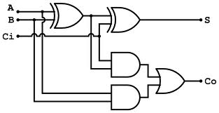
PART 6 - CIRCUIT DIAGRAM (VERSION 2) Here is a simpler
version that expresses part of CO’s circuit using the same XOR gates as used
in S. This reduces the total number of gates down from 7 to 5.
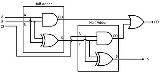
It turns out that the gates
above are actually two half adders connected together along with an OR gate.
TASK Create a full
adder. You have three options
(circuit version 1, 2 and 3)
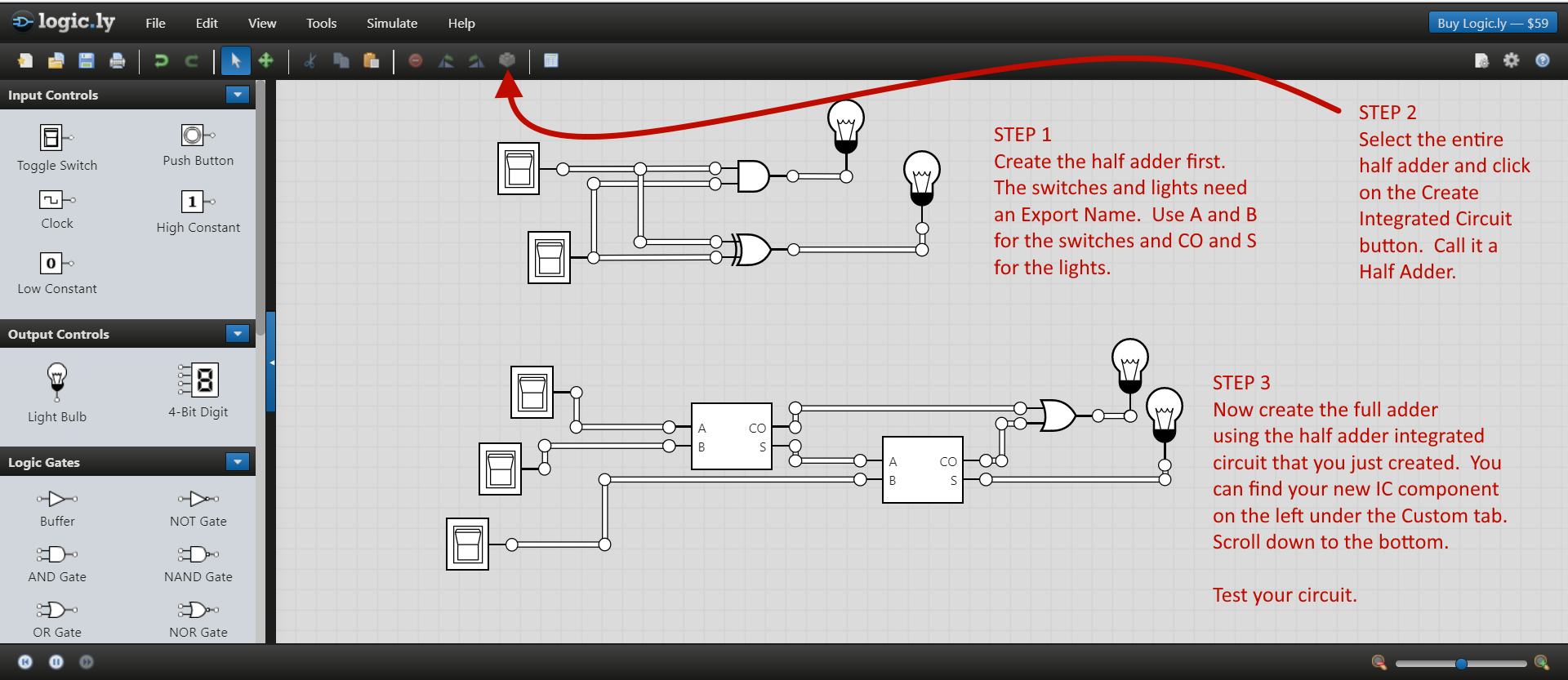
Note: For Version 3, you
need to create a custom integrated circuit in the software. You can find instructions here. TO SUBMIT A screen capture with A=1, B=0 and
CI=1. Once you have a full adder
completed. You can select all of it
and create an Full Adder integrated circuit.
(Super awesome!) Then, you can use two full adders to
add up two 2-bit numbers. Pretty
interesting stuff! |