DIGITAL DESIGN REVIEW
QUESTION 1
Connect the dots that are connected internally inside the
breadboard. Once a pattern is clear, you
do not need to continue.

QUESTION 2
Draw a voltage regulator on the breadboard below. Connect wires so that the topmost row is
positive 5 volts and the bottommost row is 0V (negative). Don’t forget to show the power source and the
wires connecting it to the regulator.

QUESTION
3
Draw the circuit below on the breadboard on the right. Your goal is to simply show that you fully
understand how to go from a circuit diagram to working with a breadboard.

QUESTION
4
What are the TTL chip numbers that contain the following gates? (You do not need to memorize these.)
NAND
NOR
NOT
AND
OR
XOR
555 Timer
QUESTION 5
Create the following circuits on the breadboard by drawing an IC with
the proper number on it. Label inputs as
A & B. Label the output with the
letter Q. Assume the breadboard is
already powered. Positive is at the top
and negative is at the bottom.
a) 0 AND 1 b)
1 NOR 1 c)
NOT (1)

QUESTION 6
Create the circuit A AND B AND C = Q on the breadboard. The inputs should not be connected to
specific value and should be labeled. The
output should be connected to an LED.

QUESTION 7
Show how to create a NOR gate using a NAND gate. You can assume the breadboard is
powered. No need to have an LED for the
output. (Look this up on the
website. You do not need to memorize
these equivalent circuits.)
QUESTION 8
Give 4 reasons why an LED in a circuit might not be lighting up as
expected.
QUESTION 9
Explain why breadboards are used to make circuits.
QUESTION
10
What is a pinout? Give an
example. Where can we find pinouts?
QUESTION
11
Draw a half adder on the breadboard below. Remember that a half adder is simply the
addition of two 1-bit numbers. There are
two outputs (to be labeled Q & R).
a)
Start with the truth table.
b)
Come up with circuits for each output.
c)
Draw the circuit on the breadboard below.

QUESTION 12
Removed from review.
QUESTION
13
Draw the circuit A XNOR B = Q (or any equivalent circuit). Label outputs.

QUESTION
14
Draw a 2 to 4 decoder on the breadboard below. Label outputs.

QUESTION
15 – TRUE OR FALSE
a)
Wires on the breadboard should run diagonally as much
as possible.
b)
Wires on the breadboard should be as long as
possible.
c)
TTL chips are Train Train
Locomotive chips.
d)
The short leg of the LED is negative.
e)
When placing the chip in the breadboard, the half
circle should be on the right.
f)
Pin numbers start at the bottom left and go up in
the counter clockwise direction.
g)
IC stands for Integrated Circuit.
h)
A capacitor is a device that can be charged and
used like a battery.
i)
Alarm clocks usually consist of 7-segment displays.
j)
A combinational circuit has no feedback.
k)
A sequential circuit has feedback.
QUESTION
16 – FILL IN THE BLANK
a)
______________ is a circuit that has n inputs and 2n
outputs. Each possible combination for
the inputs makes exactly one of the outputs 1.
b)
If a decoder has 4 inputs, it will have _____________
outputs.
c)
The 7-segment display has 2 pins labeled CA (Common
Anode). These pins are connected to the
______________ side of all the internal LEDs.
d)
The 7-segment displays are easily burnt if one
forgets to use _______________ in series with the pin labeled CA.
e)
A _____________ _____________ circuit allows us to
add two bits together.
f)
A _____________ _____________ circuit allows us to
add multiple bit numbers together. This
does require multiple copies of the circuit to be connected together.
g)
A half adder circuit has _______ inputs and _______
outputs.
h)
To add two 4-bit numbers together, we need
______________ full adder circuits.
i)
A ________________ _________________ circuits
outputs 1 if there is an odd number of 1s as input.
j)
An 8-input parity checker will output ____________
if it has the following eight inputs: 0 1 0 1 1 0 0 1.
k)
A multiplexer uses a ______________ and AND gates to route one of the input lines (specified by
control lines) to the output.
l)
A ________________ does the opposite of a
multiplexer. It routes the single input
line to the one specified output line.
m)
A diagram that shows an IC’s pin functionality (and
often the internal logic gates) is called a(n) _____________ diagram.
QUESTION
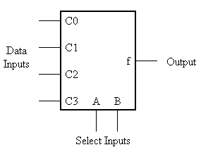
17
Consider the block diagram for a multiplexer. Explain how it works.
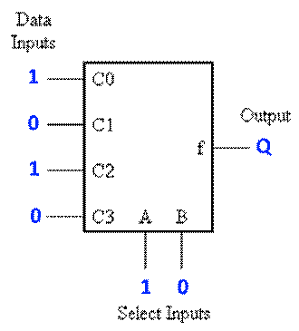
QUESTION
18
What will the value of Q be?